Circuit Design Support
We have registered schematic data for power supply integrated circuits to support your design
and development. We will continue to add products as needed, please kindly use them together.
TOREX
SEMICONDUCTOR
LTD.
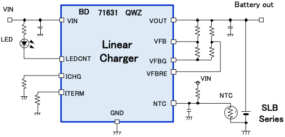
ROHM Co., Ltd.
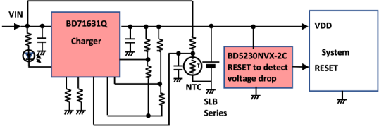
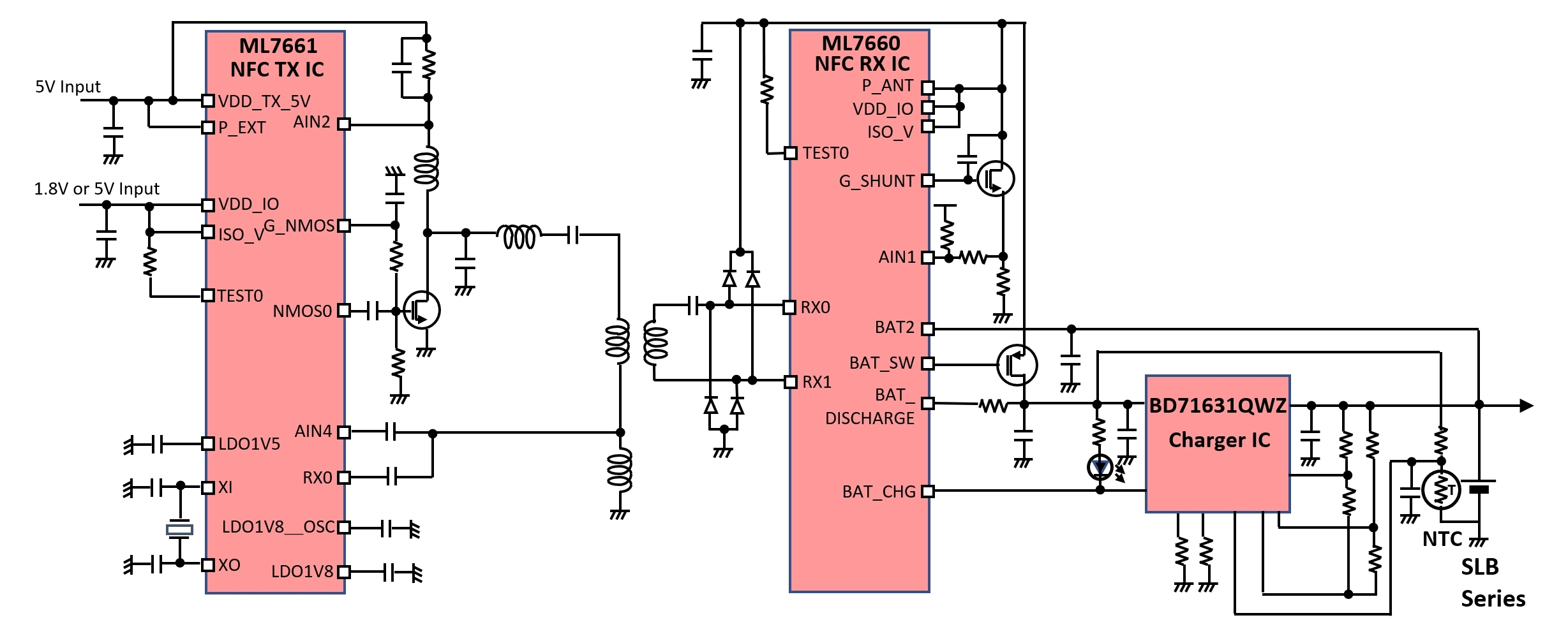
BD71631QWZ
Function
Linear Charger
Input voltage
2.9~5.5V
Charge current
1~300mA
Charger voltage
2.0~4.7V
Re charge voltage
1.8~4.7V
termination current
50μA~10mA
VOUT sink current during standby
0μA(typ)
Operating Temperature
-30~105℃
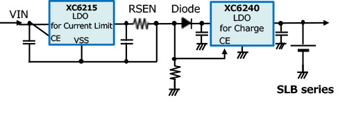
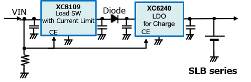
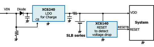
LDO for current limiting
No need
Load switch for current limiting
No need
Input diode for backflow countermeasures
No need
10 hour safety timer
Built-in
Battery temperature protection
(Additional thermistor) Built-in Battery overvoltage protection Built-in Datasheet Product HP

(Additional thermistor) Built-in Battery overvoltage protection Built-in Datasheet Product HP
Application circuit diagram
BD5230NVX-2C
Application circuit diagram
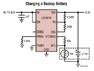
Analog Devices Inc.
LTC4079
Application circuit diagram
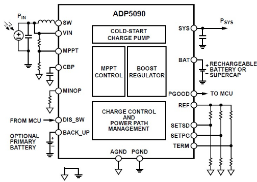
ADP5090
Function
Ultra Low Power Boost Regulator
with MPPT and Charge Management Input voltage range 80mV~3.3V Cold start voltage/power 380mV / 16μW (typ) Input peak current 100mA Programmable MPPT ratio yes Programmable shutdown point yes Programmable voltage range
for energy storage element 2.2~5.2V Quiescent current 320nA (typ; operating)
260nA (typ; sleeping) Battery current capability 800mA Regulated output no Regulated output rating current ― Optional buckup yes Temporary shutdown function yes Operating temperature -40~125℃ Datasheet
Application circuit diagram
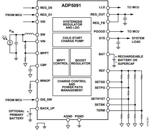
ADP5091/ADP5092
Function
Ultra Low Power Energy Harvester PMUs
with MPPT and Charge Management Input voltage range 80mV~3.3V Cold start voltage/power 380mV / 6μW (typ) Input peak current 200mA Programmable MPPT ratio yes Programmable shutdown point yes Programmable voltage range
for energy storage element 2.2~5.2V Quiescent current 510nA (typ; operating)
390nA (typ; sleeping) Battery current capability 1A Regulated output 1.5V~3.6V Regulated output rating current 150mA Optional buckup yes Temporary shutdown function yes Operating temperature -40~125℃ Datasheet
Application circuit diagram
ABLIC Inc.
S-8269B
Function
Discharge / Charge overcurrent monitoring
Discharge overcurrent detection voltage 1
0.0030 V to 0.1000 V
Discharge overcurrent detection voltage 2
0.010 V to 0.100 V
Charge overcurrent detection voltage
−0.1000 V to −0.0030 V
Load short-circuiting detection voltage
0.020 V to 0.100 V
Current consumption
4.0 uAmax.
Datasheet
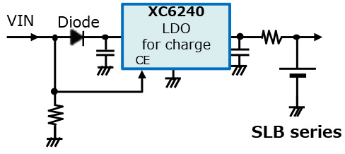
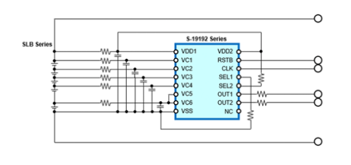
Combination circuit example
Detail
Schematic (Block Diagram)
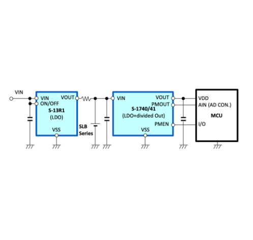
S-1740/41 Series
Function
LDO with supply voltage divided output for IoT
Operating voltage range
1.5V to 5.5V
Output voltage range
1.0V to 3.5V
(selectable in 0.05V steps) Current consumption 0.35 μA typ. (Ta=+25°C) Output voltage accuracy ±1.0%
(±15mV at 1.0V~1.45V) Output current 100 mA voltage divider output(PMOUT) VIN/2 (S-1740 series)
VIN/3 (S-1741 series) Detail information
Datasheet
Datasheet
(selectable in 0.05V steps) Current consumption 0.35 μA typ. (Ta=+25°C) Output voltage accuracy ±1.0%
(±15mV at 1.0V~1.45V) Output current 100 mA voltage divider output(PMOUT) VIN/2 (S-1740 series)
VIN/3 (S-1741 series) Detail information
Schematic (Block Diagram)
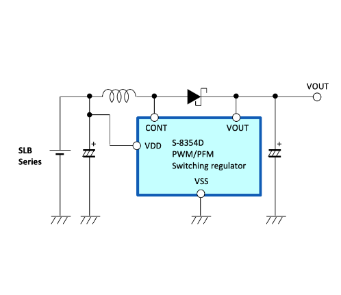
S-8354 Series
Function
High efficiency at small load step up swiching regurator
Operating voltage range
0.9 V(Iout=1 mA) to 10V
Current consumption
18.7µA typ.
(at 3.3 V, 50 kHz) Output voltage 1.5 V to 6.5 V
(VDD / VOUT separate type) Switching current 231mA (at S-8354D30) Soft start function 6ms typ. (at 50kHz) Control type PWM/PFM automatic switching Detail information Datasheet
(at 3.3 V, 50 kHz) Output voltage 1.5 V to 6.5 V
(VDD / VOUT separate type) Switching current 231mA (at S-8354D30) Soft start function 6ms typ. (at 50kHz) Control type PWM/PFM automatic switching Detail information Datasheet
Schematic (Block Diagram)
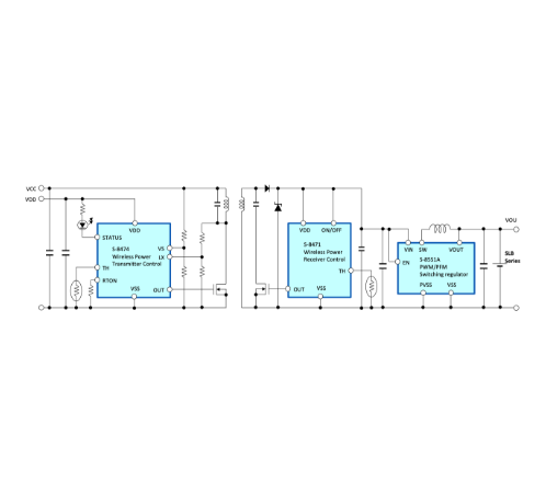
S-8474/S-8471/S-85S1A Series
Function
Wireless power supply+Step down constant voltage charging and output.
Operating voltage range
4.5 to 6.5V
(Wireless power supply) Current consumption
(S-85S1A) 260nA
(quiescent current) Output voltage
(S-85S1A) 0.7Vto2.5V,in0.05Vstep
2.6Vto3.9V,in0.1Vstep Output current 100 mA Control type
(S-85S1A) COT control Detail information
Datasheet
(Wireless power supply) Current consumption
(S-85S1A) 260nA
(quiescent current) Output voltage
(S-85S1A) 0.7Vto2.5V,in0.05Vstep
2.6Vto3.9V,in0.1Vstep Output current 100 mA Control type
(S-85S1A) COT control Detail information
Schematic (Block Diagram)
e-peas S.A.
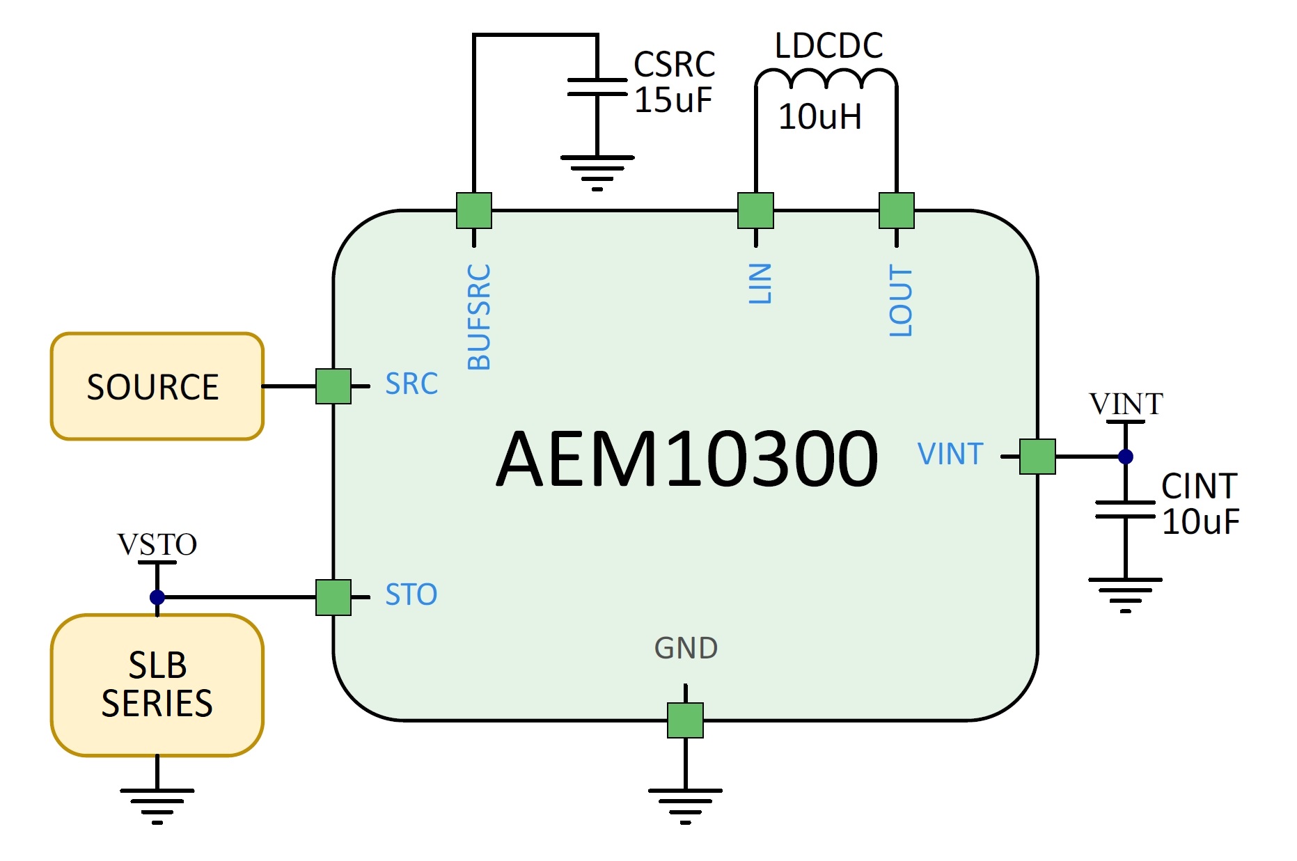
AEM10330
Function
PMIC for photovoltalic energy harvesting
Input voltage range
100mV to 4.5V
Cold start
3μW @ 275mV
Input power range
3μW to 570mW
Output current
30mA (Low power mode)
60mA (High power mode)
Selectable load voltage
from 1.2V to 3.3V MPPT Yes Package QFN40 5 x 5 mm Detail information
Architecture / How to use
Datasheet
60mA (High power mode)
Selectable load voltage
from 1.2V to 3.3V MPPT Yes Package QFN40 5 x 5 mm Detail information
Application circuit diagram

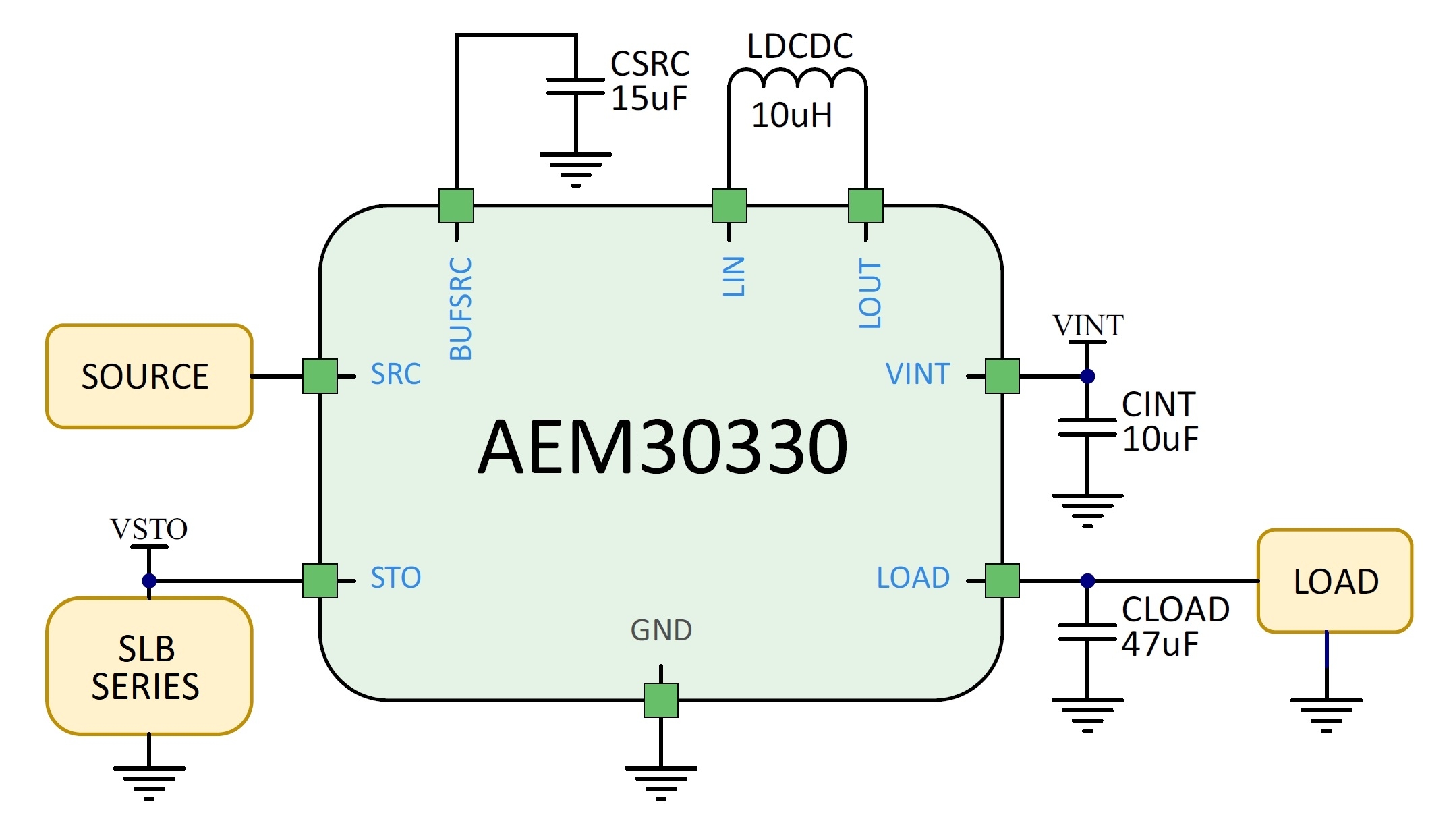
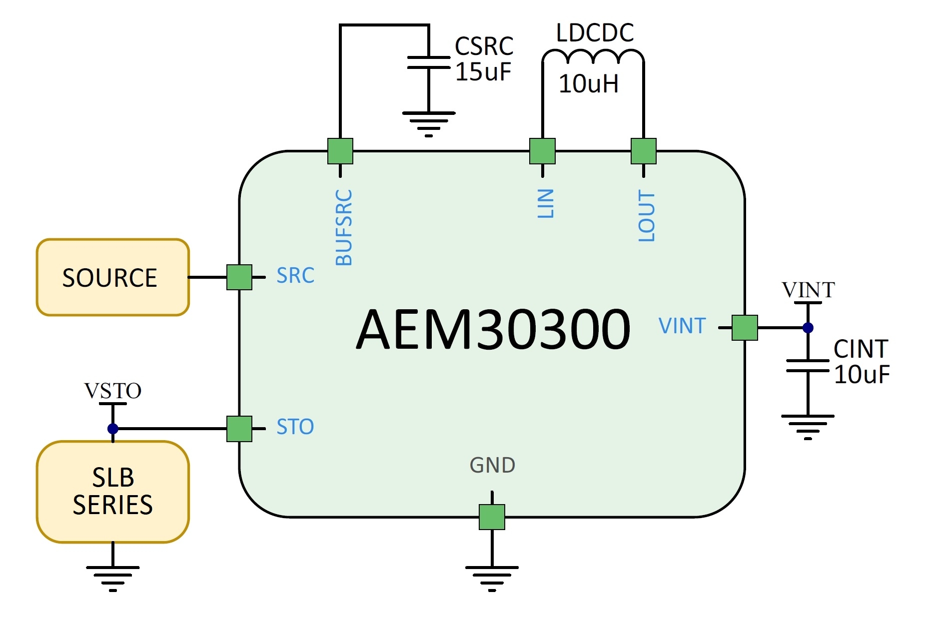
AEM30330
Application circuit diagram